Unit 5 – Part B: SEMICONDUCTORS PHYSICS
1. Obtain an expression for carrier concentration in an intrinsic semiconductor and also calculate the intrinsic carrier concentration.
1. Carrier Concentration in Intrinsic Semiconductors
Definition: The number of electrons in the conduction band per unit volume of the material or the number of holes in the valence band of the material is known as carrier concentration. It is also known as density of charge carriers.
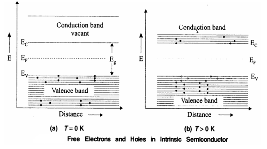
(A) Calculation of Density of Electrons in Conduction Band (\(n\))
The probability of occupancy is \(F(E) = \frac{1}{1+e^{(E-E_F)/kT}}\). Since \((E-E_F)/kT\) is very large compared to 1, the term 1 in the denominator is neglected: $$F(E) \approx e^{-(E-E_F)/kT} = e^{(E_F-E)/kT}$$
To solve, let \(x = E - E_c\). Then \(dE = dx\) and \(E = E_c + x\). The limits change from \(E_c \to \infty\) to \(0 \to \infty\). $$n = \frac{4\pi}{h^3}(2m_e^*)^{3/2} e^{(E_F-E_c)/kT} \int_{0}^{+\infty} x^{1/2} e^{-x/kT} dx$$
Using the Gamma function, \(\int_{0}^{+\infty} x^{1/2} e^{-x/kT} dx = \frac{(kT)^{3/2}\pi^{1/2}}{2}\).
(B) Calculation of Density of Holes in Valence Band (\(p\))
Using substitution \(x = E_v - E\), the integral is solved similarly using the Gamma function.
2. Calculation of Intrinsic Carrier Concentration (\(n_i\))
Multiplying the expressions for \(n\) and \(p\): $$n_i^2 = \left[ 2 \left( \frac{2\pi m_e^* kT}{h^2} \right)^{3/2} e^{(E_F - E_c)/kT} \right] \times \left[ 2 \left( \frac{2\pi m_h^* kT}{h^2} \right)^{3/2} e^{(E_v - E_F)/kT} \right]$$
Simplifying the powers and exponentials (Since \(E_c - E_v = E_g\), then \(E_v - E_c = -E_g\)): $$n_i^2 = 4 \left( \frac{2\pi kT}{h^2} \right)^3 (m_e^* m_h^*)^{3/2} e^{-E_g/kT}$$
2. Derive an expression for carrier concentration of an Extrinsic semiconductor (N–type & P-Type) and explain the variation of Fermi level with temperature.
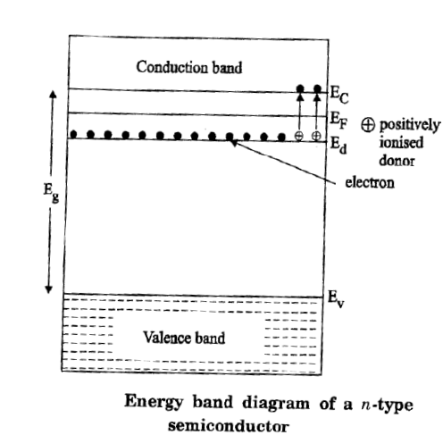
(A) Carrier Concentration in N-Type Semiconductor
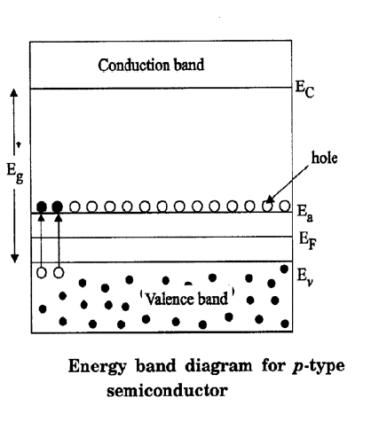
(B) Carrier Concentration in P-Type Semiconductor
(C) Variation of Fermi Level with Temperature
- At \( T = 0 \) K, the Fermi level lies exactly at the middle of the donor level (\( E_d \)) and the bottom of the conduction band (\( E_c \)): $$ E_F = \frac{E_d + E_c}{2} $$
- As temperature increases, the Fermi level decreases and moves towards the intrinsic Fermi level.
- At \( T = 0 \) K, the Fermi level lies exactly at the middle of the acceptor level (\( E_a \)) and the top of the valence band (\( E_v \)): $$ E_F = \frac{E_a + E_v}{2} $$
- As temperature increases, the Fermi level increases and moves towards the intrinsic Fermi level.
3. Describe the construction and working principle of Schottky diode. Give its advantages, disadvantages and applications.
1. Construction
A Schottky diode is formed by a junction between a metal and a semiconductor. The specific conditions for its construction are:
- Materials: It is formed when a metal with a high work function is brought into contact with an n-type semiconductor with a lower work function.
- Schottky Junction: The junction formed is called a Schottky junction.
- Terminals: The metal region acts as the anode, and the n-region acts as the cathode.
It is a unilateral device, meaning current flows only in one direction (from metal to semiconductor).
2. Working Principle
When the metal and n-type semiconductor are brought into contact:
- Fermi Level Alignment: The Fermi levels of the metal and semiconductor line up.
- Electron Transfer: Since the semiconductor has a lower work function, electrons from the conduction band of the semiconductor move to the empty energy states in the metal.
- Potential Barrier: This transfer leaves a positive charge on the semiconductor side and a negative charge on the metal side, creating a contact potential (barrier).
- Band Bending: The energy bands in the semiconductor bend upward in the direction of the electric field within the depletion region.
- Connection: The metal is connected to the positive terminal and the n-type semiconductor to the negative terminal.
- Operation: The applied external potential opposes the in-built potential. This lowers the barrier for electrons.
- Current Flow: Electrons are injected from the external circuit into the n-type semiconductor and cross into the metal. This results in a large current flow that increases exponentially with the applied voltage.
- Connection: The metal is connected to the negative terminal and the n-type semiconductor to the positive terminal.
- Operation: The external potential acts in the same direction as the junction potential.
- Depletion Region: This increases the width of the depletion region.
- Result: There is no flow of electrons from the semiconductor to the metal (only a very small current exists). Thus, the diode acts as a rectifier.
3. Advantages
- Low Capacitance: Stored charges or the depletion region is negligible, leading to very low capacitance.
- Fast Switching: Due to the negligible depletion region, the diode can immediately switch from the ON state to the OFF state.
- High Efficiency: A small voltage is sufficient to produce a large current.
- High Frequency Operation: It can operate at very high frequencies.
- Low Noise: The device produces less noise compared to conventional PN junction diodes.
4. Applications
- Rectification: Used for rectification of signals at frequencies exceeding 300 MHz.
- Switching: Used as a switching device at frequencies up to 20 GHz.
- Communication: Used in sensitive communication receivers like radars due to its low noise figure.
- Radio Frequency: Used in RF applications.
- Logic Circuits: Widely used in computer logic circuits and integrated circuits (ICs).
- Power Supplies: Used in power supply circuits.
- Signal Processing: Used in clipping and clamping circuits.
4. What is Hall Effect? Derive an expression for the Hall Voltage. Explain an experimental method used to measure the Hall Coefficient. What are the uses of Hall effect?
1. Hall Effect
Definition: When a conductor (metal or semiconductor) carrying a current (\( I \)) is placed in a perpendicular magnetic field (\( B \)), a potential difference (electric field) is produced inside the conductor in a direction normal to the directions of both the current and the magnetic field.
This generated voltage is called the Hall Voltage.
2. Derivation of Hall Voltage and Hall Coefficient
This accumulation of electrons creates a vertical electric field \( E_H \) (Hall Field). At equilibrium, the upward electric force balances the downward magnetic force: $$ eE_H = Bev $$ $$ E_H = Bv \quad \dots(1) $$
The current density is \( J_x = \frac{I_x}{bt} \). Substituting these into equation (3): $$ \frac{V_H}{t} = R_H \left( \frac{I_x}{bt} \right) B $$ $$ V_H = R_H \frac{I_x B}{b} $$ Rearranging for Hall Coefficient:
3. Experimental Method to Measure Hall Coefficient
- A semiconductor material is taken in the form of a rectangular slab of thickness \( t \) and breadth \( b \).
- A current \( I_x \) is passed through the sample along the X-axis using a battery.
- The sample is placed between the poles of an electromagnet so the magnetic field \( B \) is applied along the Z-axis (perpendicular to the plane).
- Two probes are fixed at the centers of the bottom and top faces to measure the Hall Voltage \( V_H \) developed along the Y-axis.
4. Uses of Hall Effect
- Determination of Semiconductor Type: The sign of the Hall coefficient indicates whether the semiconductor is n-type (negative) or p-type (positive).
- Calculation of Carrier Concentration: The density of charge carriers can be found using \( n = \frac{1}{e R_H} \).
- Determination of Mobility: Mobility can be calculated using electrical conductivity (\( \sigma \)) as \( \mu = \sigma R_H \).
- Magnetic Field Meter (Gauss Meter): Since \( V_H \propto B \), the Hall voltage can measure unknown magnetic fields.
- Hall Effect Multiplier: It can output a signal proportional to the product of two inputs (Current \( I \) and Field \( B \)).
5.(i): Draw the band diagram for an ohmic contact and explain its principle, theory, V-I characteristics of ohmic contact.(10)
1. Principle
An Ohmic contact is a non-rectifying contact which obeys Ohm's Law (\( V=IR \)). The resistance of the Ohmic contact should always be low (i.e., conductivity should be large). Current is conducted equally in both directions with very little voltage drop across the junction.
2. Theory
An Ohmic junction is formed when an n-type semiconductor has a higher work function than the metal (\( \phi_{semi} > \phi_{metal} \)).
Electrons move from the metal (higher energy) to the empty states in the conduction band of the semiconductor. This flow continues until the Fermi levels align.
This creates an Accumulation Region of electrons near the interface on the semiconductor side. Unlike a depletion region, this accumulation of charge carriers facilitates easy conduction.
3. Band Diagram
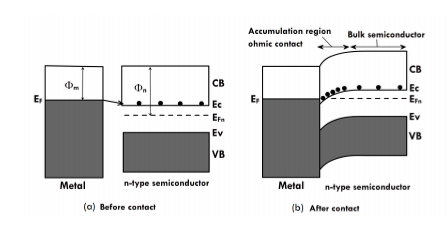 (a) Before Contact: Show Metal on left, Semiconductor on right. Metal Fermi level is higher than Semiconductor Fermi level.
(b) After Contact: The bands in the semiconductor bend downwards towards the interface. Electrons accumulate in the conduction band dip near the junction. This region is labeled "Accumulation region".
4. V-I Characteristics
Since there is no potential barrier to block the flow of electrons in either direction (due to the accumulation of carriers), the junction behaves like a resistor.
- The V-I characteristic is Linear.
- It passes through the origin.
- The slope represents the conductance of the contact.
- It follows Ohm's law: \( I \propto V \).
(ii): The Hall coefficient of certain silicon specimen was found to be 7.35*10-5m3C-1 from 100 to 400K. Determine the nature of the semiconductor. If the conductivity was found to be Ω-1 m-1, Calculate the density and mobility of the charge carrier.(6)
- Hall Coefficient (\( R_H \)) = \( 7.35 \times 10^{-5} \, m^3C^{-1} \) (Taken as negative for n-type calculation based on PDF solution context).
- Temperature Range = 100 to 400 K.
- Conductivity (\( \sigma \)) = \( 200 \, \Omega^{-1}m^{-1} \) (Value taken from PDF Problem 6).
- Charge of electron (\( e \)) = \( 1.6 \times 10^{-19} \, C \).
1. Nature of the Semiconductor
The semiconductor is an 'n-type' semiconductor.